-
Notifications
You must be signed in to change notification settings - Fork 0
6581 DACs
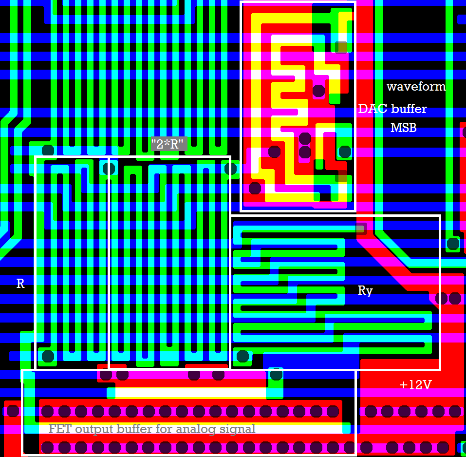
MSB of one of the waveform DACs:

West: R/2R PolySi resistor ladder of the DAC. North east: digital DAC buffer for one bit, which gives out 0V or +5V. South east: Ry, that odd pullup resistor to +12V at the output of the R/2R ladder. South: two FETs to buffer the analog output of the R/2R ladder, feeding the envelope DAC. When taking the impedance of the digital DAC buffers into account, resistor ratio for the DAC ladder is R/2.02R.
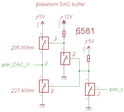
Schematic for a digital waveform DAC buffer:

Buffer is non_inverting, and the output either pulls to GND, or gives out +5V. Note, that the FET which gives out +5V at the output has a pullup to +12V at the gate. The input of those buffers are fed by the waveform selector switches.
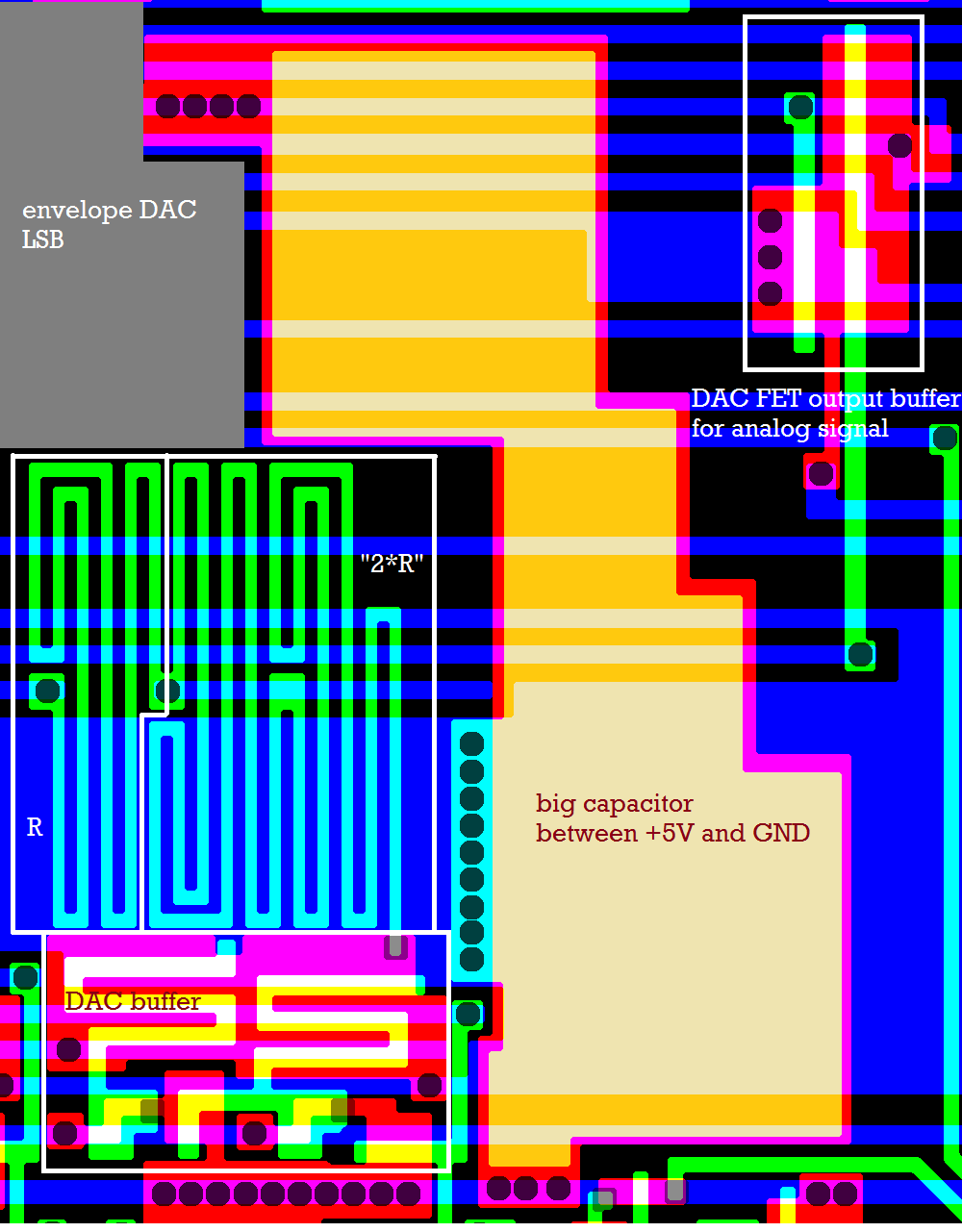
Next, the buffered analog signal from the waveform DAC enters the envelope DAC. The envelope DAC controls the amplitude of the signal. Picture from the LSB of an envelope DAC:

The digital envelope DAC buffers are controlled by the envelope generator.
Another R/2R PolySi ladder is fed by the digital envelope DAC buffers, and the analog output of the ladder at the MSB is buffered by two more FETs before it enters the selector switches.
Schematic for one bit of the digital envelope DAC buffer:

Odd thing about that buffer is: If the bit at the buffer input is 1, the buffer connects the output to the signal from the waveform DAC to the output. If the bit at the buffer input is 0, the buffer connects the output to +5V.
Note, that both FETs at the buffer output have a pullup to +12V at the gate.
When taking the output impedance of the digital envelope DAC buffers into account, resistor ratio for the ladder is R/2.02R.
Now about the switches.
The registers which control all the switches and the filter frequency DAC all have identical layout.
Schematic for one register bit:

Note: the PolySi write control lines are a bit long, so the designers added a FET to every 8 bit register as a "kludge" to meet the bus hold timing that clobbers the write control signal to GND if PHI2 =0, like with the registers in the envelope generator.
When the register bit controls analog switches, the schematic is looking like this:

And on the silicon:

East, we have a big PolySi pad that connects to a bit on the internal data bus. West, we have two analog switches, one normally open (NO) // closed, if the register bit is written with 1, one normally closed (NC) // closed, if the register is written with 0 (geometry/ratio of the FET that works as an analog switch gives the resistance of a closed switch) ...and in the middle, we have the register bit.
Now for the DAC that controls the filter frequency.

North of the DAC, we have those FETs which clobber down the write control signals to GND if PHI2 =0.
We only have 11 bits for filter frequency control in the SID, but it's a 12 bit DAC. The MSB of the DAC is nailed to '1', and there is a dead register east of the DAC MSB driver.
A closer look at a part of the PolySi resistor ladder:

Note the connection below the via in the north west corner of the picture, which ties the MSB DAC buffer input to +12V.
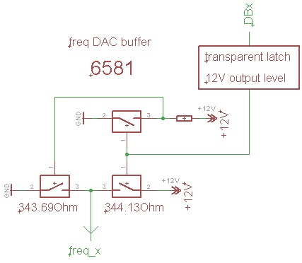
When taking the output impedance of the drivers into account, I'm getting a R/1.879R ratio. Feels strange, and somebody better check my results. Also, two of the resistances in the ladder are a little bit different from the others, I had written their values in a different color (blue instead of red) in my big schematic. The frequency control DAC feeds the gates of two FETs in the filter section which work as voltage controlled resistances for the filter integrators. Allegedly the transfer curve of those FETs isn't linear, and the designers had tinkered with that DAC trying to compensate a little bit for this. The digital frequency control DAC buffers either give out +12V at the output, or switch the output to GND.
Picture of one digital DAC buffer with register:

Schematic for the buffer:

Clock
Reset
Address Decoders
Data Bus
Registers
Oscillator
Pulse Waveform
Triangle Waveform
Noise Generator
Wave Selector
Envelope Overview
Envelope Counter
Sustain Comparator
ADSR registers
Counter Logic
Exponential Divider
LFSR15 counter
LFSR5 counter
Analog stage overview
6581 DACs
6581 Opamps
6581 Filter overview
6581 Audio output
8580 DACs
8580 Virtual ground
8580 AC Voltage divider
8580 Opamps
8580 Filter overview