-
Notifications
You must be signed in to change notification settings - Fork 0
Clock
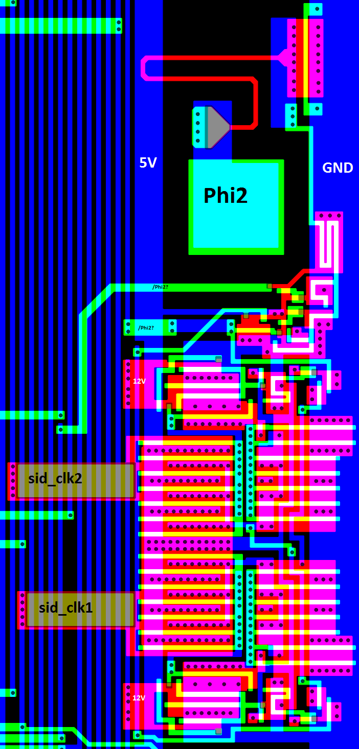
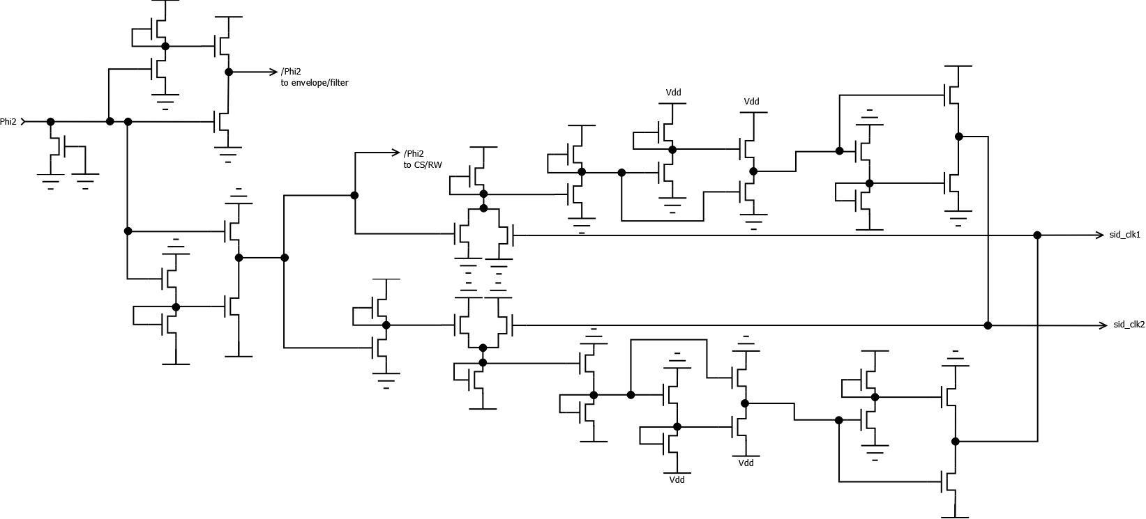
The SID chip is driven by an external phi2 clock which is internally split into two non overlapping clock lines. The clock circuitry is made of two symmetrical parts that produce two signals used to synchronize the digital logic of the chip, sid_clk2 which is high when phi2 is high and sid_clk1 which is high when phi2 is low. There are also two other lines driven by push-pull inverters that forward the inverted phi2 signal to the R/W and CS pins circuit and to the envelope and filter parts of the chip.


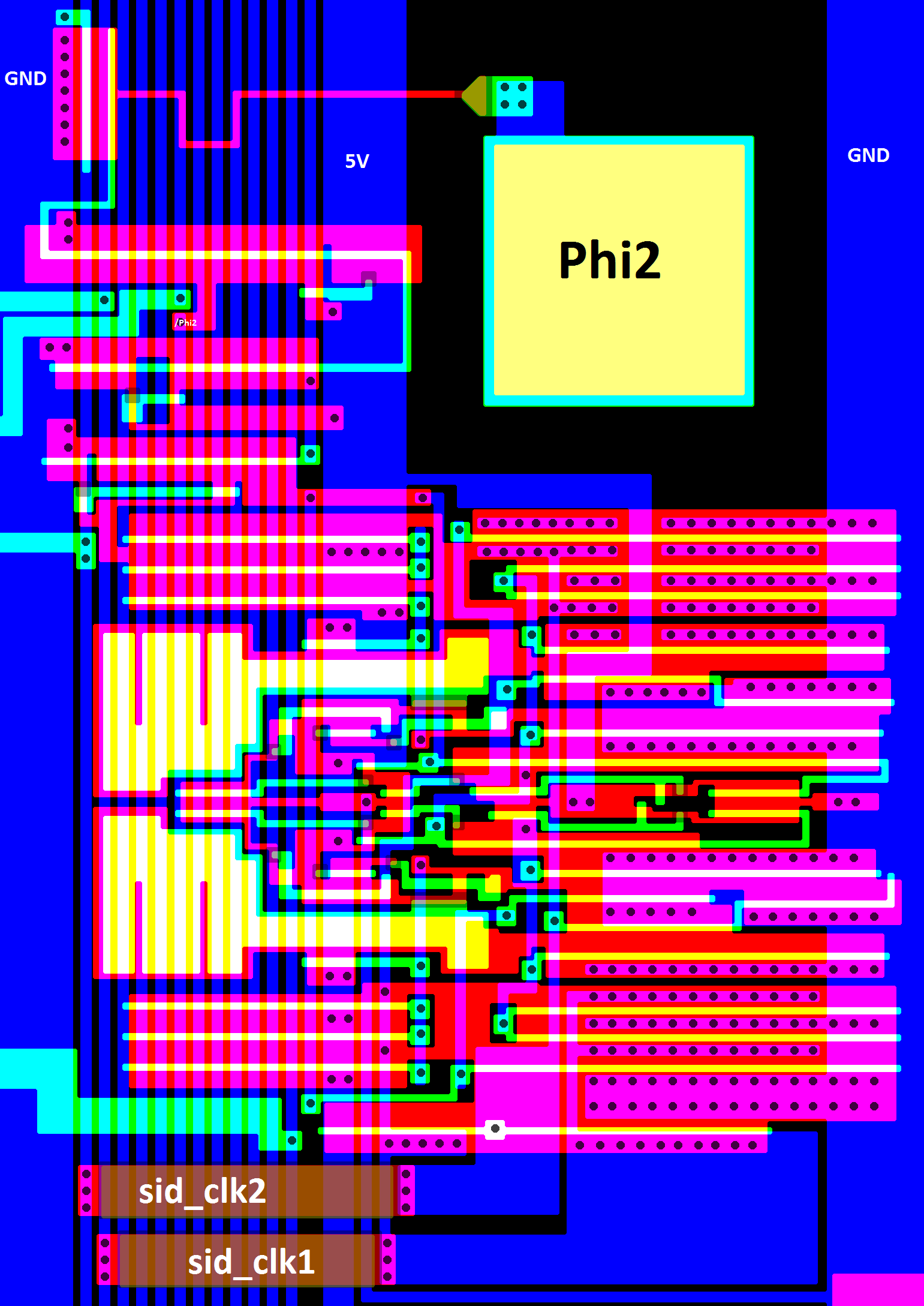
On the 8580 the clock circuit have been completely redesigned, probably to cope with the different Vdd voltage.


Clock
Reset
Address Decoders
Data Bus
Registers
Oscillator
Pulse Waveform
Triangle Waveform
Noise Generator
Wave Selector
Envelope Overview
Envelope Counter
Sustain Comparator
ADSR registers
Counter Logic
Exponential Divider
LFSR15 counter
LFSR5 counter
Analog stage overview
6581 DACs
6581 Opamps
6581 Filter overview
6581 Audio output
8580 DACs
8580 Virtual ground
8580 AC Voltage divider
8580 Opamps
8580 Filter overview