-
Notifications
You must be signed in to change notification settings - Fork 0
Pulse Waveform
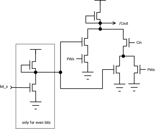
The pulse waveform is obtained by comparing the upper 12 bits of the oscillator with a programmable Pulse Width value and setting all the output bits to zero or one depending on the result of the comparison. In this picture we can see the Pulse Width register bit on the right and an adder's carry-block on the left.

The PulseWidth register bits are formed by a couple of inverters where the feedback loop is clocked by sid_clk1. The input is taken from the data bus and is enabled by the $2 line (PWLO) for the low eight bits and $3 (PWHI) for the others.

The carry calculator is the same as the one in the oscillator adder, with the inverted logic for the even bits. In order to perform a subtraction the two's complement of the pulse width value is used as input. The pw bits are taken inverted and the carry input (Cin) for the first bit is connected to Vcc (logical 1).

the resulting expression is:
/Cout = ¬((bit_x ∧ PW_x) ∨ (Cin ∧ (bit_x ∨ PW_x)))
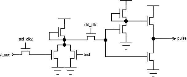
The output of the last carry calculator is then used to generate the pulse output, unless the test bit is set.

The carry output is latched at sid_clk2 and NORed with the test bit. The result is latched at sid_clk1 and used, after an inversion, for the pulse bits. The latching causes a one cycle delay in the pulse waveform with respect to the oscillator value.

When the test bit is set the pulse output is fixed at $fff.
Clock
Reset
Address Decoders
Data Bus
Registers
Oscillator
Pulse Waveform
Triangle Waveform
Noise Generator
Wave Selector
Envelope Overview
Envelope Counter
Sustain Comparator
ADSR registers
Counter Logic
Exponential Divider
LFSR15 counter
LFSR5 counter
Analog stage overview
6581 DACs
6581 Opamps
6581 Filter overview
6581 Audio output
8580 DACs
8580 Virtual ground
8580 AC Voltage divider
8580 Opamps
8580 Filter overview