-
Notifications
You must be signed in to change notification settings - Fork 0
8580 DACs
MSB of one of the waveform DACs:
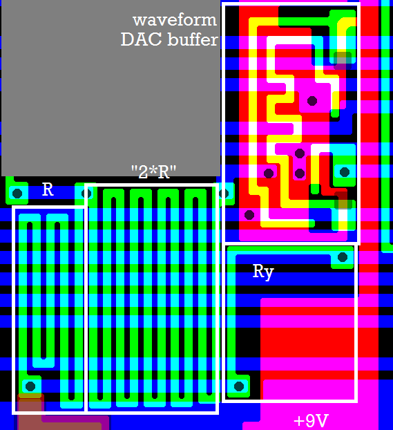
West: R/2R PolySi resistor ladder of the DAC. North east: digital DAC buffer for one bit, which gives out 0V or +5V. South east: Ry, that odd pullup resistor to +5V at the R/2R ladder. Unlike in the 6581, the output of this ladder is not buffered, and goes directly to the envelope DAC. When taking the impedance of the digital DAC buffers into account, resistor ratio for the DAC ladder is R/1.986R.
Schematic for a digital waveform DAC buffer:
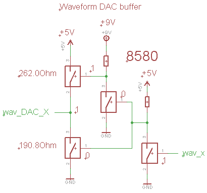
Buffer is non_inverting, and the output either pulls to GND, or gives out +5V. Note, that the FET which gives out +5V at the output has a pullup to +9V at the gate. The inputs of those buffers are fed by the waveform selector switches.
Next, the unbuffered analog signal from the waveform DAC enters the envelope DAC. The envelope DAC controls the amplitude of the signal.
Picture from the LSB of an envelope DAC:

The digital envelope DAC buffers are controlled by the envelope generator. Another R/2R PolySi ladder is fed by the digital envelope DAC buffers, and the analog output of the ladder at the MSB is directly sent to the selector switches without being buffered. The 2R end at the LSB of the ladder is tied to ca. 4.759V by a 105.36k resistor and a ca. 377.8Ohm FET (with +9V at the gate) in series. That 4.759V voltage is the "vitual ground" in the amplifier\filter section, we are getting there later.
Schematic for one bit of the digital envelope DAC buffer:

Odd thing about that buffer is: If the bit at the buffer input is 1, the buffer connects the output to the signal from the waveform DAC to the output. If the bit at the buffer input is 0, the buffer connects the output to +4.759V (virtual ground, labeled REF' in my schematic). Note, that both FETs at the buffer output have a pullup to +9V at the gate. When taking the output impedance of the digital envelope DAC buffers into account, resistor ratio for the ladder is R/1.979R.
Now about the switches.
From the logic design point of view, the registers which control all the switches and the filter frequency DAC all have identical schematics. The layout for the register bits varies a little to make better use of the space on the silicon, also size\geometry of the FET at the output might vary a little depending on the load it has to drive.
Schematic for one register bit:

Note: the PolySi write control lines are a bit long, so the designers added a FET to every 8 bit register as a "kludge" to meet the bus hold timing that clobbers the write control signal to GND if PHI2 =0, like with the registers in the envelope generator.
The game is similar like in the 6581, except for one thing: each of the switches is built from two FETs instead of just one FET.
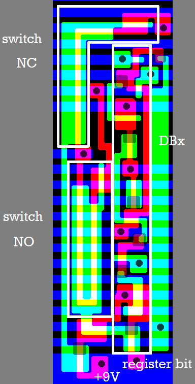
East, we have a big PolySi pad that connects to a bit on the internal data bus.
West, we have two analog switches,one normally open (NO) // closed, if the register bit is written with 1 one normally closed (NC) // closed, if the register is written with 0 Note: geometry\ratio of the FET that works as an analog switch gives the resistance of a closed switch. and in the middle, we have the register bit.
In the 6581, we had one FET working as a switch for an analog signal.
In the 8580, we have two FETs working as a single switch for an analog signal: A FET with a low impedance and a FET with a high impedance in series. This might be a trick from the designers to reduce capacitance between both ends of a switch. The FET with the higher impedance tends to be at the side of the switch that connects to an OP or such.
Note, that this trick is also used in the frequency control DACs, and maybe for resistors which don't act as a switch, too.
Schematic for a register bit plus frequency control DAC buffer:
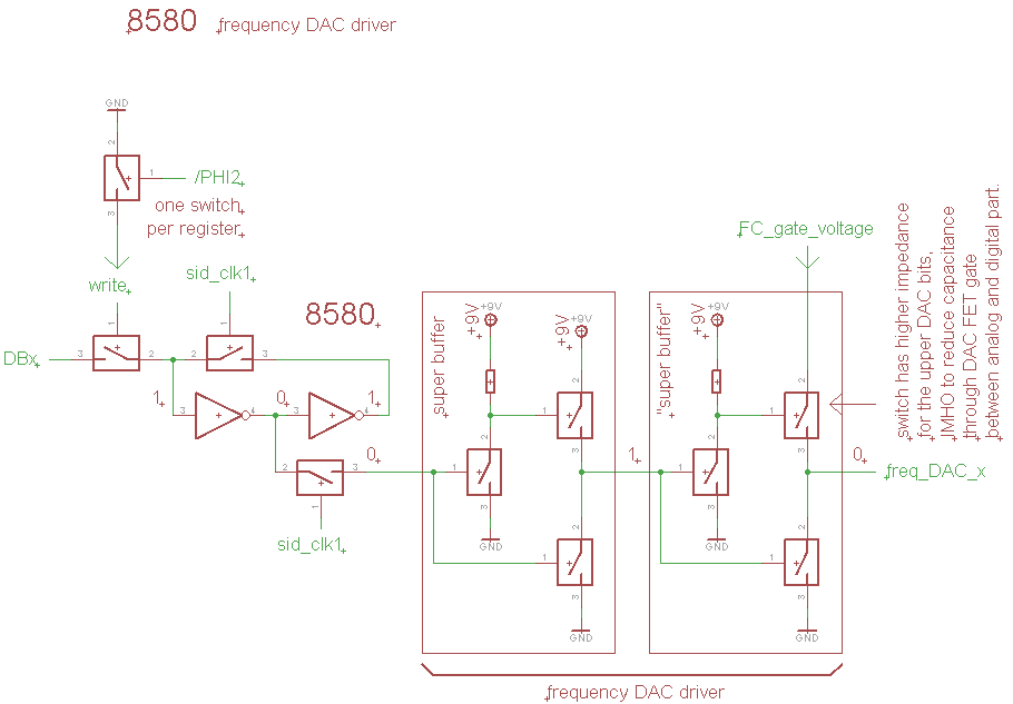
Nothing special, conceptually the DAC buffer is just a super buffer... but it's +9V powered. The output either is tied to GND, or to the gate control voltage mentioned in the previous post.
We have two identical 12 bit DACs in the 8580, which work as resistances for the filter integrators:
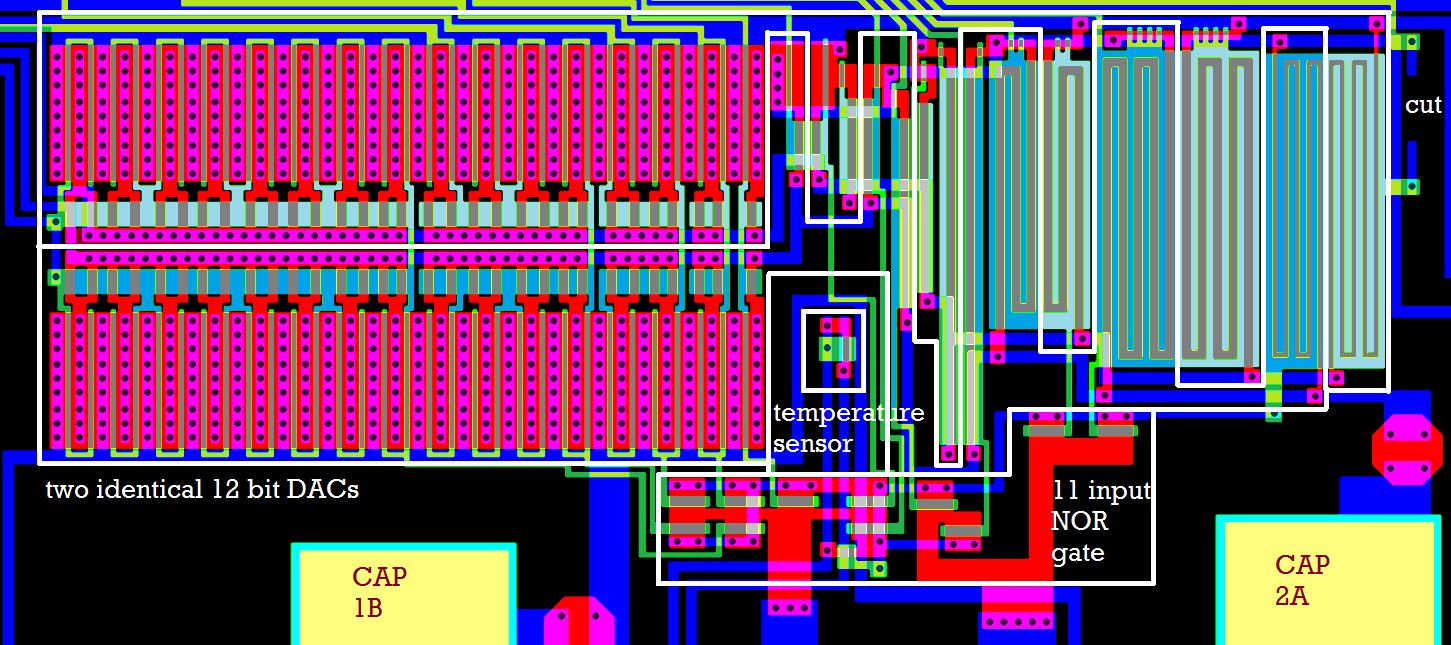
The 8580 has 11 bits for frequency control, but 12 bit DACs. If those 11 bits would be '0', the impedance of the DACs would be "infinitely high". To get around this, there is an 11 input NOR gate below the DACs sensing those 11 bits. If they are 0, the NOR gate gives the gate control voltage to the 12 bit DAC LSB.
Between the DACs and the NOR gate, we have that FET which works as a temperature sensor for the circuitry that changes the gate control voltage according to the DAC temperature.
Schematic for one of the two DACs:

Like with the other analog switches in the 8580, in the DAC we have two FETs working as a single switch for an analog signal: A FET with a low impedance and a FET with a high impedance in series. This might be a trick from the designers to reduce capacitance between both ends of a switch. The FET with the higher impedance tends to be at the side of the switch that connects to an OP or such.
For resonance control, we have two more tiny DACs and a little bit of decoding for them. That stuff is located north of the "BP feedback" OpAmp on the silicon.

Schematic:

'Gate_RR0'..'Gate_RR7' in the schematic above is just the gate voltage for the analog resonance switches R0..R7. Again two FETs of different resistance in series for every switch, and the geometry\ratio of the FETs defines the switch resistance when the switch is closed.
Clock
Reset
Address Decoders
Data Bus
Registers
Oscillator
Pulse Waveform
Triangle Waveform
Noise Generator
Wave Selector
Envelope Overview
Envelope Counter
Sustain Comparator
ADSR registers
Counter Logic
Exponential Divider
LFSR15 counter
LFSR5 counter
Analog stage overview
6581 DACs
6581 Opamps
6581 Filter overview
6581 Audio output
8580 DACs
8580 Virtual ground
8580 AC Voltage divider
8580 Opamps
8580 Filter overview